

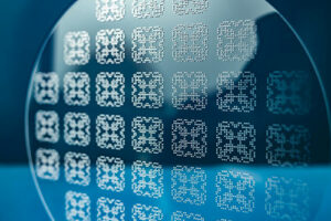
Electron beam lithography (EBL) is a versatile patterning technique based on electron beam technology that enables mask-less (“direct-write”) lithography of electron-sensitive materials. It is possible to overcome the diffraction limit of the UV lithography with sub-nm feature resolution. The machine is essentially composed by an electron column for the generation of the beam with controlled aperture, a high-precision stage for the positioning of the samples with very low stitching errors. EBL is the flexible instrument that gives fast results in the designing phase of new projects and can be used for small volume production thanks to high speed patterning.
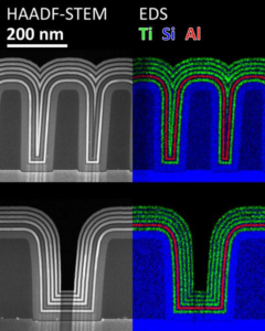
 Atomic Layer Deposition (ALD) is an advanced chemical vapour deposition technique that allows ultra-thin films to be deposited in a precisely controlled way. The precursors are sequentially inserted inside the chamber and react with the surface to be deposited autonomously in sequence. For each gas pulse in the chamber, a reaction will occur and therefore the deposition of a nanometric film will cover the surface homogeneously layer by layer. Not only does ALD provide excellent thickness control and uniformity but 3D structures can be covered with a conformal coating for high-aspect-ratio structures.
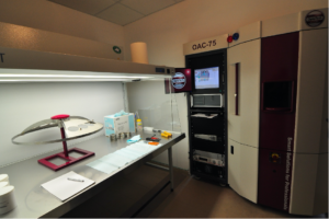
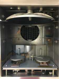 OAC-75F machine situated in CNOS laboratory of nanophotonics allows, via e-beam evaporation, the deposition of layers of different kind of materials, from oxides (as SiO2, HfO2, Al2O3), to metals (as Au, Al, Ti), to semiconductors (as Silicon), in a high vacuum chamber. This machine has been customized and optimized in order to achieve a high degree of accuracy, up to 1-2 Å in the nominal thickness, and a surface roughness of 0.1nm for most materials, in order to be able to reliably fabricate also layers with thickness at the nanometer scale. The presence of two e-beam guns and two sets of crucibles for target materials allows an efficient fabrication also of multilayer structures with two or more different materials. Furthermore, with a suitable programming of the two e-beam guns, it is possible to evaporate at the same time two different materials with different deposition rates, in order to obtain an arbitrary amorphous mixture of two materials. To guarantee a high level of adhesion and/or compactness of materials, it is possible to program the activation, before and during the deposition, of a plasma ion source based on Argon and/or Oxygen gases. The large vacuum chamber allows to allocate, for the same deposition process, several substrates of different shape and dimensions, from standard silicon wafers to optical fibers, providing a very good level of uniformity thanks to the rotation of the dome hosting the substrates.
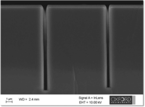
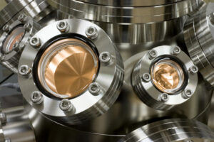 Reactive Ion Etching – RIE – is a chemical etching technique that uses a plasma to remove a material from a substrate. The plasma is generated by an electromagnetic field in a high vacuum chamber starting from precursors in a gaseous state. The ions present in the plasma chemically attack the surface and react with it. The result is a very uniform surface and it is possible to control the process very well thanks to various parameters involved in the process, such as temperature, flow of gases.
The use of this machine is intended for the effective and selective removal of material from substrates on which deposition and / or lithography operations have already been performed. The system allows to work on conventional planar substrates and on unconventional substrates such as optical fibers. For example, it is possible to attach the glass of which the optical fiber is made in a suitable way downstream of a lithographic process. In this way only the exposed areas will be etched and it will therefore be possible to create nanostructures with very high aspect ratios.
Reactive Ion Etching – RIE – is a chemical etching technique that uses a plasma to remove a material from a substrate. The plasma is generated by an electromagnetic field in a high vacuum chamber starting from precursors in a gaseous state. The ions present in the plasma chemically attack the surface and react with it. The result is a very uniform surface and it is possible to control the process very well thanks to various parameters involved in the process, such as temperature, flow of gases.
The use of this machine is intended for the effective and selective removal of material from substrates on which deposition and / or lithography operations have already been performed. The system allows to work on conventional planar substrates and on unconventional substrates such as optical fibers. For example, it is possible to attach the glass of which the optical fiber is made in a suitable way downstream of a lithographic process. In this way only the exposed areas will be etched and it will therefore be possible to create nanostructures with very high aspect ratios.
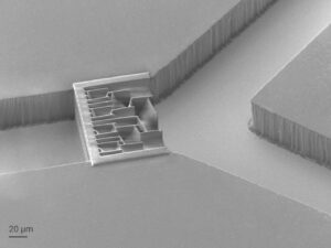
 The femtosecond laser system, a proper laser laboratory on an optical table, is a versatile system that allows ablation of glass, metals and polymers, and photolithography using the common photoresist. Thanks to the four-axis (XYZ and one of rotation R), we can process several types of substrates – from planar surfaces to unconventional surfaces, like optical fiber tip – with extreme resolution and accuracy avoiding sample damaging.
Among the various fields of application, some examples are:
The femtosecond laser system, a proper laser laboratory on an optical table, is a versatile system that allows ablation of glass, metals and polymers, and photolithography using the common photoresist. Thanks to the four-axis (XYZ and one of rotation R), we can process several types of substrates – from planar surfaces to unconventional surfaces, like optical fiber tip – with extreme resolution and accuracy avoiding sample damaging.
Among the various fields of application, some examples are:
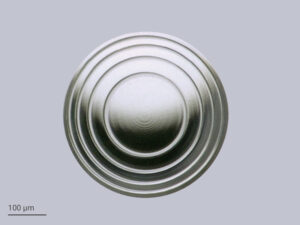
 The two-photon polymerization system (2PP) is a maskless lithography system, designed for the fabrication of high-resolution 2D and 3D structures. This machine has a galvanomentric system that allows us to manufacture nanostructures with desired geometry straight on both planar and non-planar surfaces. It has an X and Y resolution of 400nm and a scan speed of up to 100mm / s.
The 2PP system has different application area:
Laser system: NIR femtosecond laser
Type of resins: PDMS, biocompatible and non-cytotoxic according to ISO 10993-5, with high refractive index (n = 1.62) and low autofluorescence.